Frontiers of Data and Computing ›› 2021, Vol. 3 ›› Issue (5): 4-27.
doi: 10.11871/jfdc.issn.2096-742X.2021.05.001PID:21.86101.2/JFDC.ISSN.2096.742X.2019.01.012
CSTR:32002.14.jfdc.issn.2096.742X.2019.01.012
• Special Issue: Problems and Counter measures in the field of In fomation Tellnology in China • Previous Articles Next Articles
XU Haitao1,*( ),PENG Lianmao2,*()
Received:2021-10-01
Online:2021-10-20
Published:2021-11-24
Contact:
XU Haitao,PENG Lianmao
E-mail:htxu@bicic.cn;lmpeng@pku.edu.cn
XU Haitao,PENG Lianmao. Carbon-Based Integrated Circuit Technology: Development and Forecast[J]. Frontiers of Data and Computing, 2021, 3(5): 4-27.
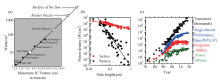
Fig.1
The Power Wall for silicon chips"


Fig.2
The Memory Wall for silicon chips Single-thread"

Fig.3
Ideal channels for logic devices - carbon nanotubes"
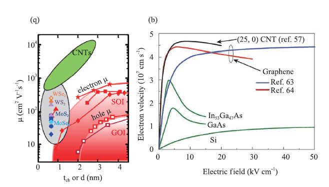

Fig.4
Carbon nanotube arrays prepared by CVD and purified by thermocapillary method"
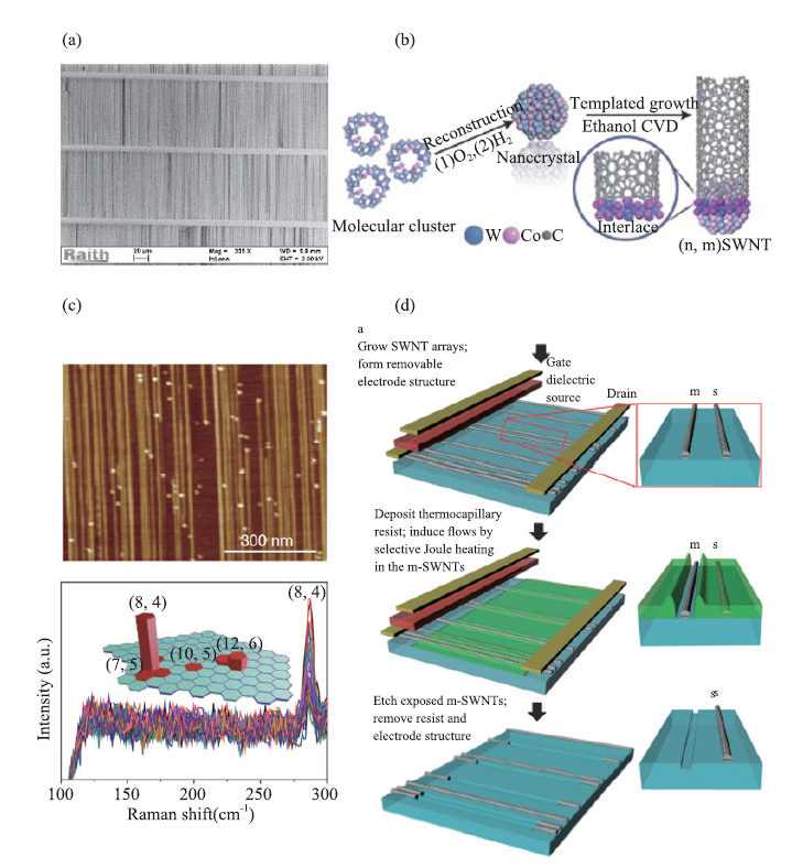

Fig.5
General process of dispersion and sorting of SWNTs via conjugated polymer"
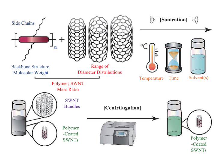

Fig.6
Most used conjugated polymer for s-SWNT sorting"
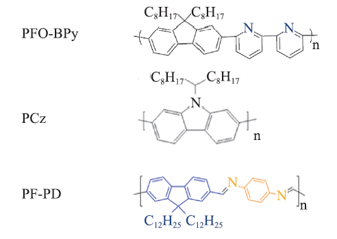
Fig.7
Alignment of carbon nanotubes"
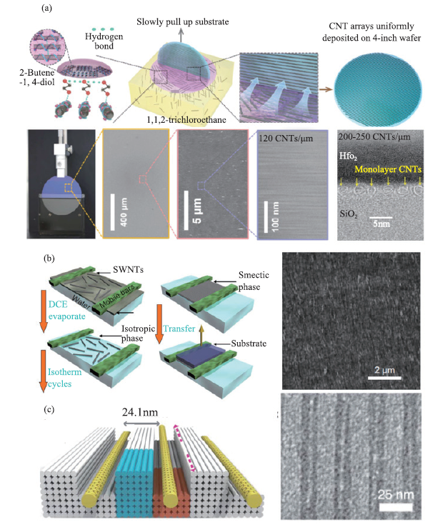
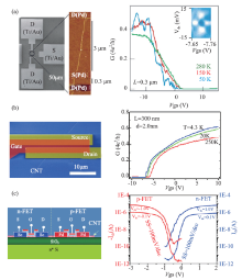
Fig.8
Doping-free carbon nanotube CMOS"
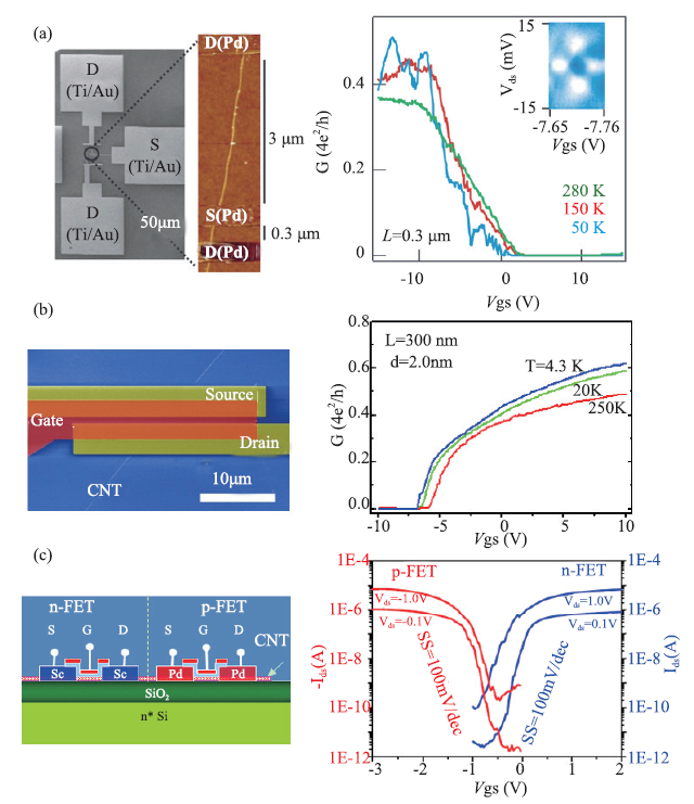
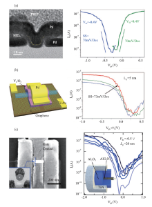
Fig.9
Extremely scaling CNT FET with planar top gate (TG) and gate-all-around (GAA) structure"


Fig.10
Ballistic CNT FET"
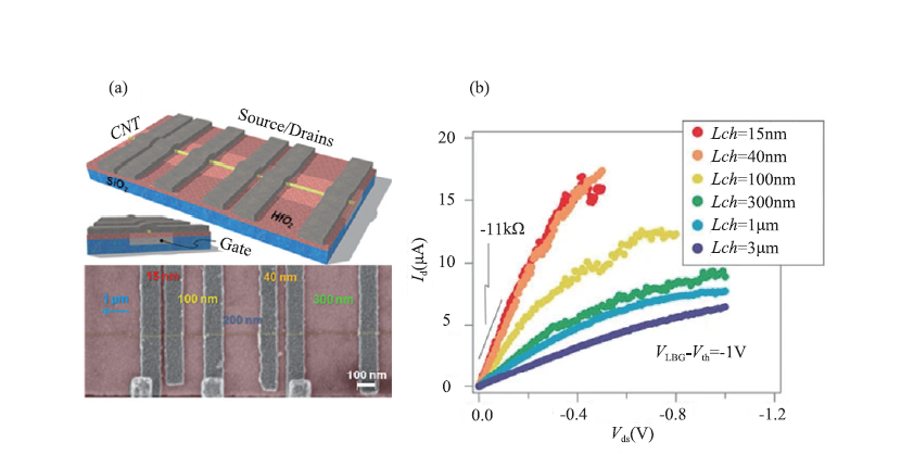

Fig.11
Contact length scaling of CNT FETs"
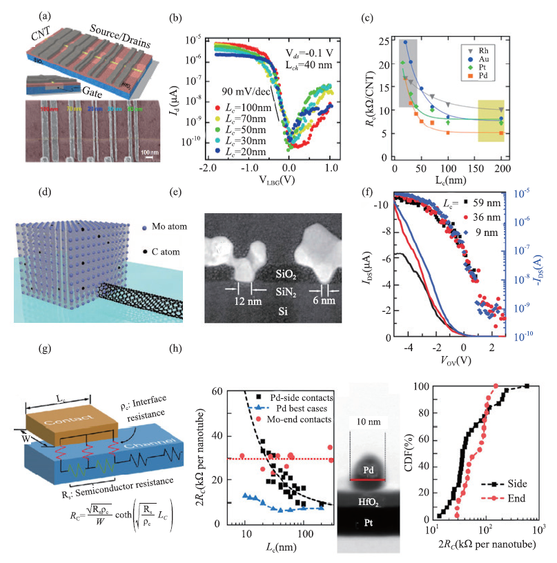
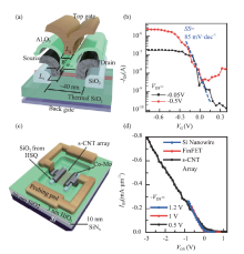
Fig.12
Smallest CNT FET- 40 nm footprint"


Fig.13
Fabrication of high-k gate dielectric for CNT FETs"
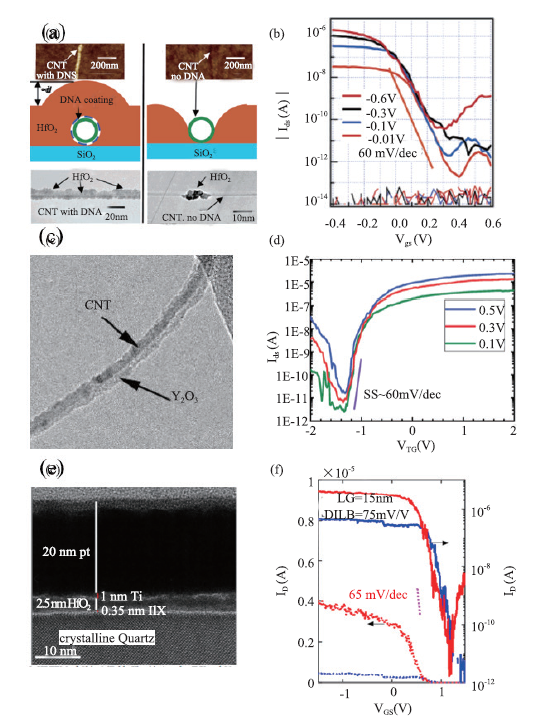

Fig.14
Carbon nanotube Risk-V microprocessor"
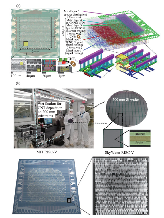

Fig.15
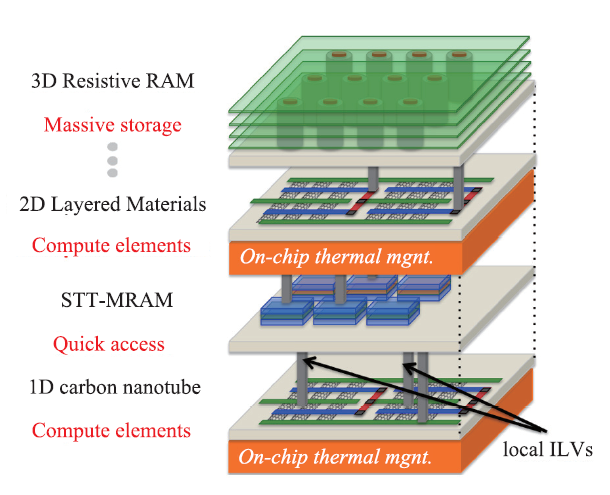
Carbon-based monolithic 3D integration"
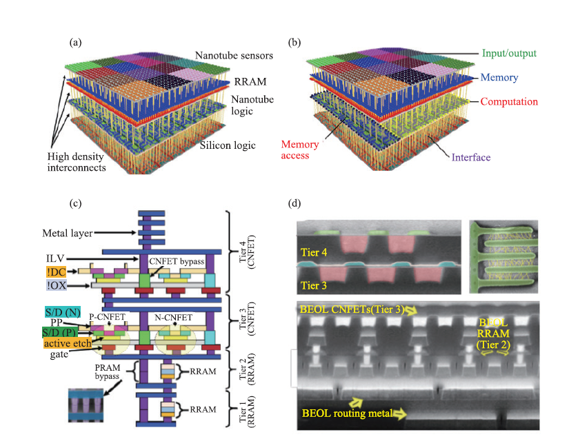

Fig.16
High speed carbon nanotube 5-stage oscillators"
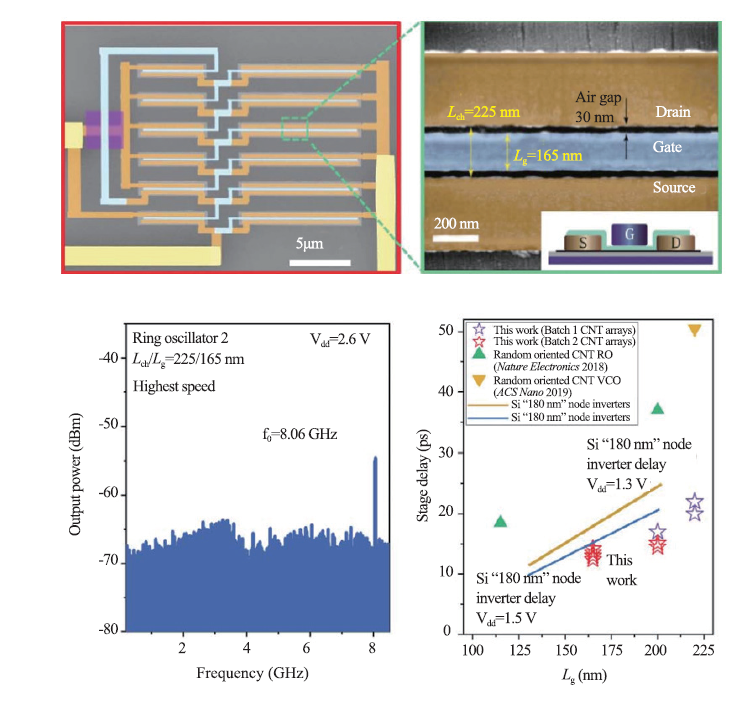

Fig.17
Passivation of Sc contacted CNT NMOS"
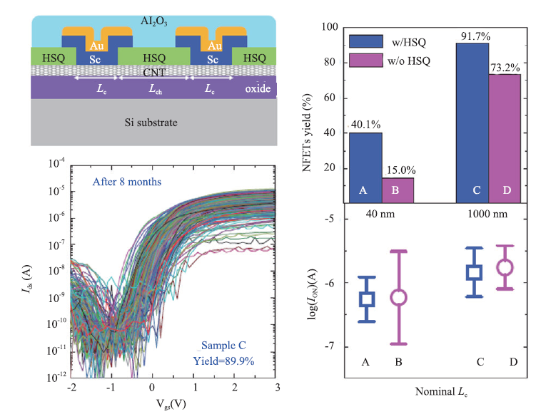

Fig.18
CNT NMOS with electrostatic doping"
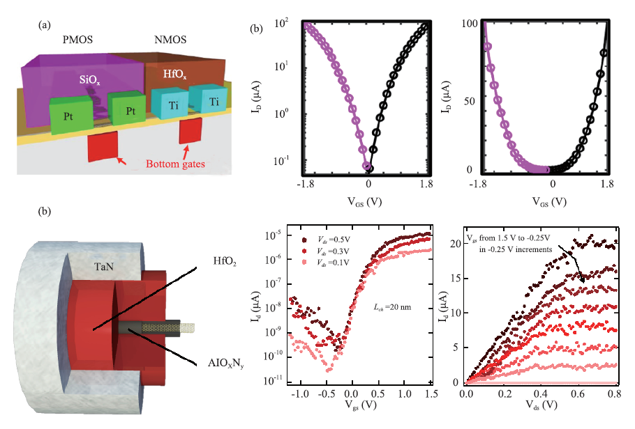

Fig.19
Cabon-Based monolithic 3D integration"
| [1] |
Cao Q. Carbon nanotube transistor technology for More-Moore scaling[J]. Nano Res. 2021, 14:3051-3069.
doi: 10.1007/s12274-021-3459-z |
| [2] | Ronald G. Dreslinski, Michael Wieckowski, et al. Near threshold computing: overcoming performance degrad-ation from aggressive voltage Scaling[D]. In Proc. ISCA Workshop on Energy-Efficient Design, 2009. |
| [3] | H.-S. Philip Wong. Carbon Nanotube Digital Nanosy-stems[D]. PKU CNT Workshop, 2015. |
| [4] | Tathagata Srimani, G. Hills, M.M. Shulaker, et al. Heter-ogeneous integration of BEOL logic and memory in a commercial foundry: multi-tier complementary carbon nanotube logic and resistive RAM at a 130 nm node[J]. VLSI, 2020, 9265083. |
| [5] | Aaron Franklin. Nanomaterials in transistors: From high-performance to thin-film applications[J]. Science, 2015, 349:6249 |
| [6] | Frank Schwierz. Graphene transistors[J]. Nat. Nano-technol., 2010, 5:487. |
| [7] |
F Yang et al. Chirality-specific growth of single-wall- ed carbon nanotubes on solid alloy catalysts[J]. Nature, 2014, 510:522-524.
doi: 10.1038/nature13434 |
| [8] |
Shuchen Zhang, Zhang Jin, et al. Arrays of horizontal carbon nanotubes of controlled chirality grown using designed catalysts[J]. Nature, 2017, 543:234-238.
doi: 10.1038/nature21051 |
| [9] |
Jin S., Dunham S., Song J. et al. Using nanoscale thermocapillary flows to create arrays of purely semicon-ducting single-walled carbon nanotubes[J]. Nature Nanotech., 2013, 8:347-355.
doi: 10.1038/nnano.2013.56 |
| [10] |
A. A. Green, M. C. Hersam. Nearly single-chirality single-walled carbon nanotubes produced via orthogonal iterative density gradient ultracentrifugation[J]. Adv. Mater., 2011, 23:2185.
doi: 10.1002/adma.v23.19 |
| [11] | S. Ghosh, S. M. Bachilo, R. B. Weisman. Advanced sorting of single-walled carbon nanotubes by nonlin-ear density-gradient ultracentrifugation[J]. Nat. Nanote-chnol., 2010, 5:443. |
| [12] |
J. A. Fagan, M. Zheng, et al. Isolation of specific small-diameter single-wall carbon nanotube species via aque-ous two-phase extraction[J]. Adv. Mater., 2014, 26:2800.
doi: 10.1002/adma.v26.18 |
| [13] |
H. Gui, J. K. Streit, M. Zheng, et al. Redox sorting of carbon nanotubes[J]. Nano Lett., 2015, 15:1642.
doi: 10.1021/nl504189p |
| [14] |
Huiliang Wang, Zhenan Bao. Conjugated polymer sorting of semiconducting carbon nanotubes and their electronic applications[J]. Nano Today, 2015, 10:737-758.
doi: 10.1016/j.nantod.2015.11.008 |
| [15] |
Qiu S., Li Q. W., et al. Solution-processing of high-purity semiconducting single-walled carbon nanotubes for electronics devices[J]. Adv. Mater., 2019, 31:1800750.
doi: 10.1002/adma.v31.9 |
| [16] |
Liyuan Liang, Wanyi Xie, Song Qiu, Qingwen Li, et al. High-efficiency dispersion and sorting of single-walled carbon nanotubes via non-covalent interactions[J]. J. Mater. Chem. C, 2017, 5:11339-11368.
doi: 10.1039/C7TC04390B |
| [17] |
Darryl Fong, Alex Adronov. Recent developments in the selective dispersion of single-walled carbon nanotubes using conjugated polymers[J]. Chem. Sci., 2017, 8:7292-7305.
doi: 10.1039/c7sc02942j pmid: 29163880 |
| [18] |
Mistry K.S B.A. Larsen, and J.L. Blackburn. High-yield dispersions of large-diameter semiconducting single-walled carbon nanotubes with tunable narrow chirality distributions[J]. ACS Nano, 2013, 7(3):2231-2239.
doi: 10.1021/nn305336x pmid: 23379962 |
| [19] |
Gu J.T., J. Han, D. Liu, X.Q. Yu, L.X. Kang, S. Qiu, H.H. Jin, H.B. Li, et al. Solution-processable high-purity semiconducting SWCNTs for large-area fabrication of high-performance thin-film transistors[J]. Small, 2016, 12(36):4993-4999.
doi: 10.1002/smll.201600398 |
| [20] |
Liu L, Peng LM. et al. Aligned, high-density semicon-ducting carbon nanotube arrays for high-performance electronics[J]. Science, 2020, 368:850-856.
doi: 10.1126/science.aba5980 |
| [21] |
Lei T, Chen X, Pitner G, Wong HS, Bao Z. Removable and recyclable conjugated polymers for highly selective and high-yield dispersion and release of low-cost carbon nanotubes[J]. J. Am. Chem. Soc., 2016, 138(3):802-805.
doi: 10.1021/jacs.5b12797 |
| [22] |
Park H., Afzali A., Han SJ. et al. High-density integr-ation of carbon nanotubes via chemical self-assembly[J]. Nature Nanotech., 2012, 7:787-791.
doi: 10.1038/nnano.2012.189 |
| [23] |
Sun W, Shen J, Yin P. et al. Precise pitch-scaling of carbon nanotube arrays within three-dimensional DNA nanotrenches[J]. Science, 2020, 368(6493):874-877.
doi: 10.1126/science.aaz7440 |
| [24] |
Cao Q., Han Sj., Tulevski G. et al. Arrays of single-walled carbon nanotubes with full surface coverage for high-performance electronics[J]. Nat. Nanotechnol., 2013, 8:180-186.
doi: 10.1038/nnano.2012.257 |
| [25] |
Jinkins K. R., Chan J., Jacobberger R. M., Berson A., Arnold M. S. Substrate‐wide confined shear alignment of carbon nanotubes for thin film transistors[J]. Adv. Electron. Mater., 2019, 5:1800593.
doi: 10.1002/aelm.v5.2 |
| [26] |
Yongho Joo, Michael S. Arnold, Padma Gopalan et al. Dose-controlled, floating evaporative self-assembly and alignment of semiconducting carbon nanotubes from organic solvents[J]. Langmuir, 2014, 30(12):3460-3466.
doi: 10.1021/la500162x pmid: 24580418 |
| [27] |
He X., Gao W., Xie L. et al. Wafer-scale monodomain films of spontaneously aligned single-walled carbon nanotubes[J]. Nat. Nanotechnol., 2016, 11:633-638.
doi: 10.1038/nnano.2016.44 |
| [28] |
Katherine R. Jinkins, Padma Gopalan, Michael S. Arnold, et al. Nanotube alignment mechanism in floating evaporative self-assembly[J]. Langmuir, 2017, 33:13407-13414.
doi: 10.1021/acs.langmuir.7b02827 pmid: 29058446 |
| [29] |
Shi H., Ding L., Zhong D. et al. Radiofrequency transistors based on aligned carbon nanotube arrays[J]. Nat. Electron. 2021, 4:405-415.
doi: 10.1038/s41928-021-00594-w |
| [30] |
Katherine R. Jinkins, Padma Gopalan, Michael S. Arnold, et al. Aligned 2D carbon nanotube liquid crystals for wafer-scale electronics[J]. Sci. Adv., 2021, 7:eabh0640.
doi: 10.1126/sciadv.abh0640 |
| [31] |
Javey A., Guo J., Wang Q., Lundstrom M., and Dai H. J. Ballistic carbon nanotube fieldeffect transistors[J]. Nature, 2003, 424:654-657.
doi: 10.1038/nature01797 |
| [32] | Javey A., Wang Q., Kim W., and Dai H. Advancements in complementary carbon nanotube field-effect transistors[J]. IEDM, 2003, 1269387. |
| [33] |
Zhihong Chen, Phaedon Avouris et al. The role of metal-nanotube contact in the performance of carbon nanotube field-effect Ttransistors[J]. Nano Lett., 2005, 5(7):1497-1502.
pmid: 16178264 |
| [34] |
Zhang Z, Liang X, Wang S, et al. Doping-free fabrication of carbon nanotube based ballistic CMOS devices and circuits[J]. Nano Lett, 2007, 7:3603-3607.
doi: 10.1021/nl0717107 |
| [35] |
Zhiyong Zhang, Lianmao Peng et al. Almost Perfectly Symmetric SWCNT-Based CMOS Devices and Scaling[J]. ACS Nano., 2009, 3(11):3781-3787.
doi: 10.1021/nn901079p |
| [36] |
Lee C. S.; Pop E.; Franklin A. D.; Haensch W.; Wong H. S. P. A compact virtual-source model for carbon nanotube FETs in the sub-10-nm regime—Part I: Intrinsic elements[J]. IEEE Trans. Electron Devices, 2015, 62:3061-3069.
doi: 10.1109/TED.2015.2457453 |
| [37] |
Chenguang Qiu, Zhiyong Zhang, Lianmao Peng, et al. Scaling carbon nanotube complementary transistors to 5-nm gate lengths[J]. Science, 2017, 355:271-276.
doi: 10.1126/science.aaj1628 pmid: 28104886 |
| [38] |
Aaron D, Franklin, Wilfried Haensch et al. Carbon Nanotube Complementary Wrap-Gate Transistors[J]. Nano Lett., 2013, 13:2490-2495.
doi: 10.1021/nl400544q pmid: 23638708 |
| [39] |
Franklin A D, Chen Z. Length scaling of carbon nanotube transistors[J]. Nat. Nanotechnol., 2010, 5:858-862
doi: 10.1038/nnano.2010.220 pmid: 21102468 |
| [40] |
Berger H. H. Models for contacts to planar devices[J]. Solid State Electron. 1972, 15:145-158.
doi: 10.1016/0038-1101(72)90048-2 |
| [41] |
Solomon P. M. Contact resistance to a one-dimensional quasi-ballistic nanotube/wire[J]. IEEE Electron Device Lett., 2011, 32:246-248.
doi: 10.1109/LED.2010.2095821 |
| [42] |
Gregory Pitner, H.-S. Philip Wong, et al. Low-tem-perature side contact to carbon nanotube transistors: resistance distributions down to 10 nm contact length[J]. Nano Lett., 2019, 19:1083-1089.
doi: 10.1021/acs.nanolett.8b04370 pmid: 30677297 |
| [43] |
Cao Q.; Han S. J.; Haensch W. et al. End-bonded contacts for carbon nanotube transistors with low, size-independent resistance[J]. Science, 2015, 350:68-72.
doi: 10.1126/science.aac8006 |
| [44] | Tang J. S., Cao Q., Han S. J. et al. Carbon nanotube complementary logic with low-temperature processed end-bonded metal contacts[J]. IEDM, 2016, 7838350. |
| [45] |
Cao Q., Tersoff J., Han S. J. et al. Carbon nanotube tr-ansistors scaled to a 40-nanometer footprint[J]. Science, 2017, 356:1369-1372.
doi: 10.1126/science.aan2476 |
| [46] |
Lu Y, Bangsaruntip S, Wang X, et al. DNA function-alization of carbon nanotubes for ultrathin atomic layer deposition of high κ dielectrics for nanotube transistors with 60 mV/Decade switching[J]. J. Am. Chem. Soc., 2006, 128:3518-3519.
doi: 10.1021/ja058836v |
| [47] |
Wang Z, Xu H, Zhang Z, et al. Growth and performance of yttrium oxide as an ideal high-κ gate dielectric for carbon-based electronics[J]. Nano Lett., 2010, 10:2024-2030.
doi: 10.1021/nl100022u |
| [48] | G. Pitner, Z. Zhang, Q. Lin, et al. Sub-0.5 nm Interfacial Dielectric Enables Superior Electrostatics: 65 mV/dec Top-Gated Carbon Nanotube FETs at 15 nm Gate Length[J]. IEDM 2020, 9371899. |
| [49] |
Shulaker M M, Hills G, Patil N, et al. Carbon nanotube computer[J]. Nature, 2013, 501:526-530.
doi: 10.1038/nature12502 |
| [50] |
Yang Y, Ding L, Peng LM, et al. High-Performance Complementary Transistors and Medium-Scale Integrated Circuits Based on Carbon Nanotube Thin Films[J]. ACS Nano, 2017, 11:4124-4132.
doi: 10.1021/acsnano.7b00861 |
| [51] |
Hills G, Lau C, Max M, Shulaker, et al. Modern mic-roprocessor built from complementary carbon nanotube transistors[J]. Nature, 2019, 572:595-602.
doi: 10.1038/s41586-019-1493-8 |
| [52] |
Bishop M. D.; Hills G; M.; Shulaker M. M. et al. Fabrication of carbon nanotube field-effect transistors in commercial silicon manufacturing facilities[J]. Nat. Electron., 2020, 3, 492-501.
doi: 10.1038/s41928-020-0419-7 |
| [53] | Shulaker MM, Wong HSP, Mitra S, et al. Monolithic 3D integration of logic and memory: carbon nanotube FETs, resistive RAM, and silicon FETs[J]. IEDM, 2014, 7047120. |
| [54] |
Shulaker M. M., Hills G., Wong H. S. P., et al. Threedi-mensional integration of nanotechnologies for computing and data storage on a single chip[J]. Nature, 2017, 547:74-78.
doi: 10.1038/nature22994 |
| [55] |
Wu TF, Li H, Wong HSP, Shulaker MM, Mitra S. et al. Hyperdimensional Computing Exploiting Carbon Nano-tube FETs, Resistive RAM, and Their Monolithic 3D Integration[J]. IEEE J. Solid-State Circuits, 2018, 53:3183-3196.
doi: 10.1109/JSSC.2018.2870560 |
| [56] | T Srimani, G Hills, C Lau, M Shulaker. Monolithic Three-Dimensional Imaging System: Carbon Nanotube Computing Circuitry Integrated Directly Over Silicon Imager[J]. VLSI, 2019, 8776514. |
| [57] |
Zhong D., Zhang Z., Ding L. et al. Gigahertz integrated circuits based on carbon nanotube films[J]. Nat. Electron., 2018, 1:40-45.
doi: 10.1038/s41928-017-0003-y |
| [58] | Tang J., Farmer D.B., Bangsaruntip S. et al. Contact engineering and channel doping for robust carbon nano-tube NFETs[J]. VLSI-TSA, 2017, 7942478. |
| [59] |
Lau C., Srimani T., Bishop M. D., Hills G., Shulaker M. M. Tunable n-type doping of carbon nanotubes through engineered atomic layer deposition HfOx films[J]. ACS Nano, 2018, 12:10924-10931.
doi: 10.1021/acsnano.8b04208 |
| [60] |
L. S. Liyanage, H.-S. Philip Wong, et al. VLSI-Compat-ible Carbon Nanotube Doping Technique with Low Work- Function Metal Oxides[J]. Nano Lett., 2014, 14(4):1884-1890.
doi: 10.1021/nl404654j |
| [61] | H.-S. Philip Wong. The Next Technology for 21st Century Computing[J]. PKU CNT Workshop, 2017. |
| [1] | CHEN Lei,ZHAO Congpeng,GE Jie,ZUO Xuan. Overview of Integrated Circuit Technology and Industry Development Practice and Innovation Development Trend Global [J]. Frontiers of Data and Computing, 2021, 3(5): 55-64. |
| [2] | YU Li,SHENG Yingjie,XU Jinglong,SUI Xiufeng. A Study on the Bottlenecks Technologies of Integrated Circuit Industry in China from the Patent Analysis Perspective [J]. Frontiers of Data and Computing, 2021, 3(5): 40-54. |
| Viewed | ||||||
|
Full text |
|
|||||
|
Abstract |
|
|||||